Chinese Scientists Discovered Revolutionary Method to Create Flexible Diamond Membranes for Electronics

Scientists from Hong Kong and mainland China have developed a groundbreaking technique to transform diamonds—the hardest natural material—into ultrathin, flexible membranes. This innovative approach not only promises to accelerate the commercial viability of diamond-based technology but also paves the way for its widespread application in electronics, photonics, and beyond.
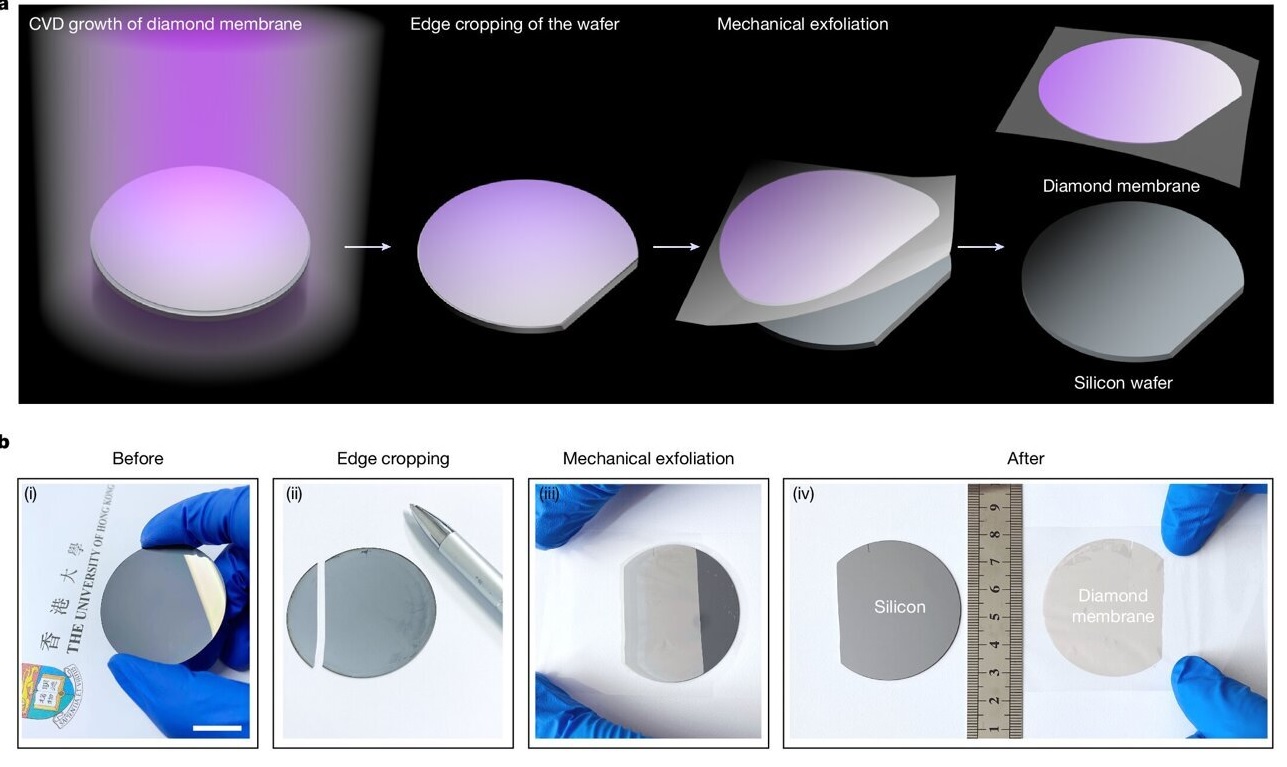
The new process, detailed in the peer-reviewed journal Nature, allows for the rapid production of diamond membranes just 1 micrometer thick—thinner than a human hair—at a fraction of the cost and time required by previous methods. Researchers have already achieved the creation of a 2-inch (5 cm) diamond wafer within 10 seconds, with plans to scale up production to 12-inch wafers.
The Breakthrough Method
Traditionally, ultrathin diamonds were either sliced from bulk material or grown on a substrate and later separated using chemical processes. These methods, however, faced significant limitations:
- Slicing bulk diamonds produced membranes too small for industrial applications.
- Growing diamonds on a substrate was time-intensive and yielded rough surfaces, rendering them incompatible with microfabrication.
The new process starts by growing a diamond membrane on a silicon substrate. The wafer edge is then cropped to expose a side of the membrane. A tape is applied on top of the membrane and peeled off at an angle to separate it from the substrate without cracking. This simple, single-step method is cost-effective and compatible with existing semiconductor manufacturing technologies.
Applications in Electronics
Diamond’s unique properties, including its exceptional thermal conductivity—five times higher than copper—make it an ideal candidate for cooling high-performance electronics. The flexible diamond membranes could serve as heat spreaders to enhance the efficiency and lifespan of processors, semiconductor lasers, and electric vehicles. Additionally, these membranes can be integrated into diamond-based electronics like field-effect transistors and wearable devices, revolutionizing the field of flexible and robust electronics.
Scalability and Commercialization
The team, comprising researchers from the University of Hong Kong, Peking University’s Dongguan Institute of Opto-Electronics, and Shenzhen’s Southern University of Science and Technology, has applied for patents in semiconductor hubs worldwide, including China, the US, Europe, Korea, Japan, and Taiwan. They aim to bridge the gap between lab-scale production and industrial manufacturing.
Co-lead author Lin Yuan, a professor of mechanical engineering at HKU, highlighted that making diamond into a thin layer drastically enhances its flexibility. According to Yuan, “If its thickness is halved, its flexibility increases by almost an order of magnitude.” The method could theoretically be adapted to other materials as well.
The researchers plan to launch a start-up to commercialize the technology, beginning with testing lines in Hong Kong and Shenzhen. These lines will demonstrate scalability before transitioning to mass production with support from investors.
Future Implications
This breakthrough heralds a potential “diamond era” in technology. With its unparalleled properties and adaptability to existing manufacturing processes, the flexible diamond membrane could significantly enhance electronic devices' performance and durability while opening doors to new innovations in wearable and high-performance electronics.


